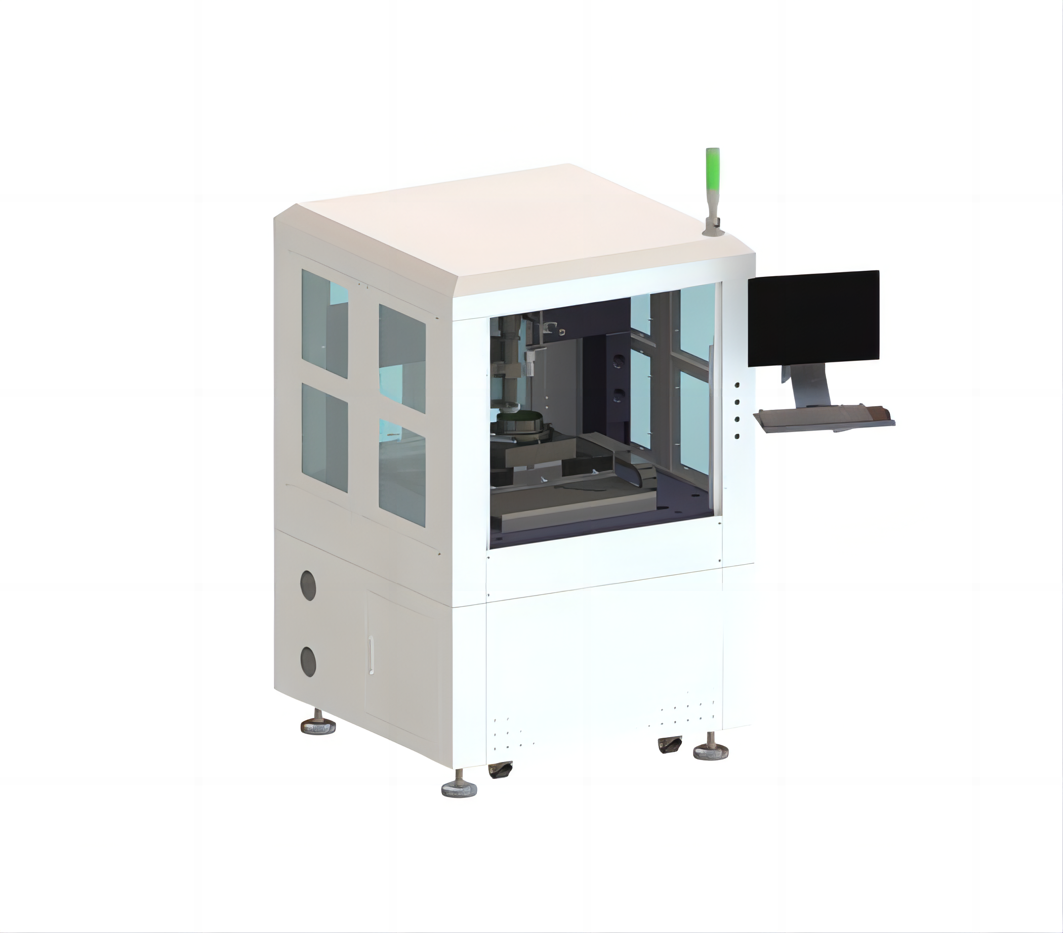
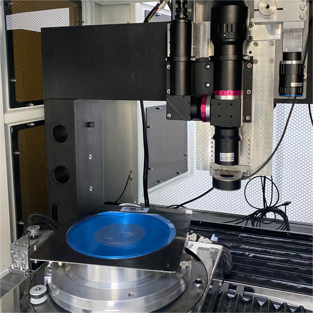
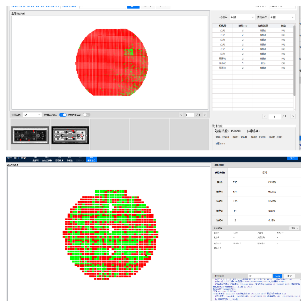
Bright-field and dark-field wafer surface inspection using high-resolution imaging based on three modes: image algorithm, detection model and anomaly detection, and provides statistical analysis.
2D Inspection accuracy
um
1
UPH
pcs/h
60
Escape
ppm
≤50
Advanced Algorithm
AI large scale model and small model cooperation, support for model training methods based on defective and non-defective; support for intelligent annotation and sample generation based on large sacle models, to solve the rapid on-line under the sample imbalance scenario; support for incremental learning mode to control the size of the sample set and improve the speed of the model iteration; support for parallel and concurrent processing modes.
Functions for data statistics and analyses
Used for inspection and production process data statistics, provides a variety of Kanban templates; for the specified defect types or specified time period, provides a variety of yield statistics; provides a variety of data saving interface, production process traceability; for industrial scenarios, supports flexible and free configuration of the display unit, statistical indicators, the results of the query, export, upload logic; integration of a unified, visual multi-machine hardware interface debugging tools, so that the debugging process is more convenient.
Algorithmic features
We can detect contamination correctly in complex background images; we can eliminate defects with specific characteristics; we can automatically generate needle mark masks, eliminate the location of needle marks, and catch defects outside the needle marks.